The quest for the ultimate display technology has long been a battle between brilliance and efficiency. While Micro LED promises unparalleled contrast and longevity, its path to mass adoption has been hindered by challenges in brightness
The quest for the ultimate display technology has long been a battle between brilliance and efficiency. While Micro LED promises unparalleled contrast and longevity, its path to mass adoption has been hindered by challenges in brightness, efficiency, and cost. Today, a groundbreaking material innovation is shattering these barriers. This article delves into a pivotal advancement: GaN-on-Silicon Micro LED technology achieving a remarkable 3x brightness improvement over traditional sapphire-based approaches.
This leap is not merely an incremental gain; it represents a fundamental shift in how we manufacture light at the microscopic scale. By transitioning from expensive sapphire substrates to scalable silicon wafers, engineers have unlocked new potentials in photonic design and thermal management. We will explore the core technical principles behind this brightness surge, its profound implications for display performance across industries, and the transformative impact it has on the commercial viability of Micro LED, paving the way for its arrival in consumer electronics.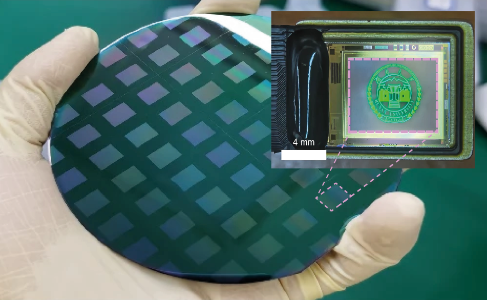
The Silicon Substrate Revolution: Unlocking Photonic Efficiency
At the heart of this breakthrough lies a simple yet profound substrate swap. Conventional Micro LEDs are typically grown on sapphire, a material with a significant lattice mismatch to Gallium Nitride (GaN). This mismatch creates crystal defects that trap electrons and holes, causing them to recombine non-radiatively—essentially generating heat instead of light. This intrinsic inefficiency caps the potential light output.
Growing GaN on silicon wafers, a process perfected for power electronics, presents a superior alternative. While challenges like lattice mismatch and thermal expansion differences exist, advanced buffer layers have now mitigated these issues. The key benefit is superior crystal quality and the ability to design more efficient photon extraction structures directly into the epitaxial layers. Silicon allows for the etching of precise photonic crystals and sidewall geometries that guide a greater percentage of generated photons out of the LED structure, rather than being lost internally. This fundamental improvement in light extraction efficiency is the primary driver behind the tripled brightness, turning more electrical energy into visible light.
Beyond Brightness: Cascading Benefits for Display Performance
The 3x brightness leap is the headline, but its ripple effects redefine display capabilities. First, it enables stunning high dynamic range (HDR) performance even at smaller pixel pitches. Micro LEDs can now achieve the extreme peak brightness required for specular highlights while maintaining deep blacks, all at lower drive currents. This reduces power consumption and heat generation, addressing two critical constraints for compact devices like AR glasses and smartwatches
.
Secondly, the enhanced efficiency directly translates to improved longevity and reliability. Operating at lower current densities for the same light output reduces quantum efficiency droop and minimizes thermal stress on the microscopic diodes. This means displays can maintain their peak brightness and color accuracy for tens of thousands of hours with minimal degradation. Furthermore, the higher intrinsic brightness provides designers with greater flexibility for optical systems, such as in projection or waveguide-based AR, where light loss is a major hurdle. The performance gain thus permeates every aspect of the visual experience, from efficiency and stability to ultimate luminance.
Catalyzing Commercial Viability: From Lab to Market
The shift to GaN-on-Silicon is as much an economic breakthrough as a technical one. Silicon wafers are larger, cheaper, and more abundant than sapphire, leveraging the vast manufacturing ecosystem of the semiconductor industry. This compatibility with existing CMOS fabrication lines allows for monolithic integration—the possibility of growing Micro LED pixels directly atop silicon driver wafers. This approach promises to eliminate the massive transfer and bonding challenges of the "pick-and-place" method, which is a major cost and yield bottleneck.
By dramatically improving performance while simultaneously lowering cost structures, this technology accelerates the roadmap for Micro LED adoption. Applications that were previously constrained by brightness or cost—such as consumer-grade augmented reality visors, ultra-bright automotive HUDs, and large-scale direct-view video walls—now become commercially feasible. It moves Micro LED from a premium-only technology towards a scalable solution poised to challenge OLED and mini-LED across multiple market segments, truly heralding the era of next-generation displays.
In conclusion, the achievement of a 3x brightness improvement in GaN-on-Silicon Micro LEDs marks a watershed moment for display technology. It successfully marries the superior optical properties of GaN with the economic and engineering virtues of silicon substrates, solving fundamental issues of efficiency and scalability in one stroke. This advancement not only unlocks unprecedented visual performance in terms of brightness and HDR but also paves a credible path to mass production. As the industry overcomes the final integration hurdles, we stand on the brink of a display revolution where stunning visual fidelity, exceptional efficiency, and commercial accessibility finally converge.


