In the relentless pursuit of visual technology breakthroughs, a formidable alliance is taking shape in Japan. Kyocera Corporation, a global leader in advanced ceramics and components, has announced a significant collaboration with multiple Japanese universities
In the relentless pursuit of visual technology breakthroughs, a formidable alliance is taking shape in Japan.
Kyocera Corporation, a global leader in advanced ceramics and components, has announced a significant collaboration with multiple Japanese universities. Their shared mission is to pioneer next-generation semiconductor-based display technologies. This partnership moves beyond incremental improvements, aiming to fundamentally redefine how displays are created and function.
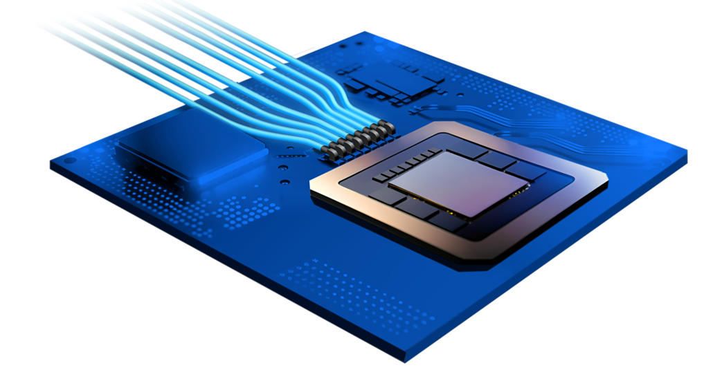
The initiative targets the core limitations of current OLED and LCD screens, focusing on micro-LED and novel semiconductor-driven solutions. By merging Kyocera's expertise in materials science and precision manufacturing with the cutting-edge research from academic institutions, this collaboration is poised to unlock innovations for future applications. This article delves into the strategic rationale, the key technological frontiers, and the profound potential impact of this ambitious venture on industries ranging from consumer electronics to augmented reality.
The Strategic Imperative: Bridging Industry and Academia
Kyocera's decision to partner with universities is a calculated strategic move, essential for tackling the monumental challenges of next-gen displays. Unlike conventional corporate R&D, which often focuses on near-term product cycles, this collaboration taps into the foundational research and blue-sky thinking prevalent in academia. Universities provide a pipeline of novel ideas and a deep understanding of fundamental physics and material properties at the nanoscale.
For Kyocera, this partnership is not merely about outsourcing research. It is a symbiotic exchange. The company brings to the table its unparalleled expertise in fine ceramics, semiconductor packaging, and mass-production scalability—critical competencies often beyond the scope of a university lab. Together, they form a complete innovation chain: from theoretical discovery and proof-of-concept at the university level, to engineering refinement and commercialization pathways guided by Kyocera. This model accelerates development by de-risking early-stage research and ensuring it is grounded in practical manufacturing realities.
Core Technological Frontiers Under Exploration
The collaboration is likely centered on several pivotal technological frontiers where semiconductor integration is key. A primary focus is undoubtedly micro-LED technology, which promises superior brightness, efficiency, and longevity compared to OLED. The immense challenge lies in the "mass transfer" process—placing millions of microscopic LED chips onto a substrate with perfect yield. Kyocera's precision engineering capabilities in micro-assembly and substrate materials are crucial here.
Another frontier involves novel semiconductor materials and processes for light emission and control. Research may explore:
-
Using gallium nitride (GaN) or other compound semiconductors on unconventional, potentially flexible, substrates.
-
Integrating display driver and control circuitry directly into the display pixel structure for faster response and higher density.
-
Developing new photonic crystals or quantum dot enhancements using advanced ceramic filters and layers.
These efforts aim to create displays that are not just sharper, but also more durable, energy-efficient, and capable of new form factors.
Envisioning the Future Impact Across Industries
The successful fruition of this R&D alliance will send ripples far beyond the smartphone and television markets. The development of robust, ultra-high-performance semiconductor-based displays is a foundational enabler for the next wave of digital innovation. In augmented and virtual reality (AR/VR), such displays are the critical bottleneck; they require, extreme brightness for outdoor use, and low latency to prevent user discomfort. This collaboration directly targets those needs.
Furthermore, the technology could revolutionize automotive displays, creating dashboard and windshield interfaces that are perfectly readable in all lighting conditions. In healthcare, ultra-reliable and high-contrast displays could advance surgical visualization and diagnostic equipment. Even public infrastructure and smart cities could benefit from ultra-durable, sunlight-readable digital signage. By solving the core material and integration challenges today, Kyocera and its academic partners are essentially building the visual interface for tomorrow's most transformative technologies.
Kyocera'shttps://tss-serviceonline.com/ university partnerships represent a profound investment in the substrate of future innovation—literally and figuratively. By fusing deep academic research with industrial-scale engineering prowess, this initiative tackles the formidable technical hurdles preventing next-generation displays from mainstream adoption. The focus on semiconductor-based solutions, from micro-LEDs to novel material integrations, promises to yield displays with unprecedented performance, durability, and efficiency. As this collaboration progresses, it will not only strengthen Japan's position in advanced electronics but also supply the critical visual components that will define the next decade of AR, automotive, and digital interaction. The future of display is being written today, in the synergy between corporate vision and academic exploration.


