In the relentless pursuit of sleeker, more immersive electronic devices, the display is often the final frontier. Manufacturers are locked in a battle to eliminate bezels, reduce weight, and deliver pristine image quality, all while maintaining durability and responsiveness. A significant technological leap in this arena has arrived from Kyocera Corporation. The company's announcement of its new in-cell touch display technology
In the relentless pursuit of sleeker, more immersive electronic devices, the display is often the final frontier. Manufacturers are locked in a battle to eliminate bezels, reduce weight, and deliver pristine image quality, all while maintaining durability and responsiveness. A significant technological leap in this arena has arrived from Kyocera Corporation. The company's announcement of its new in-cell touch display technology, which integrates touch sensors directly into the LCD cell, promises to redefine design paradigms. This innovation is not merely an incremental upgrade; it represents a fundamental shift in display architecture, targeting the core challenges of modern device design. This article delves into the mechanics of Kyocera's breakthrough, exploring how it enables thinner and lighter form factors, unlocks superior visual fidelity, and ultimately, shapes the future of user interaction with our most essential gadgets.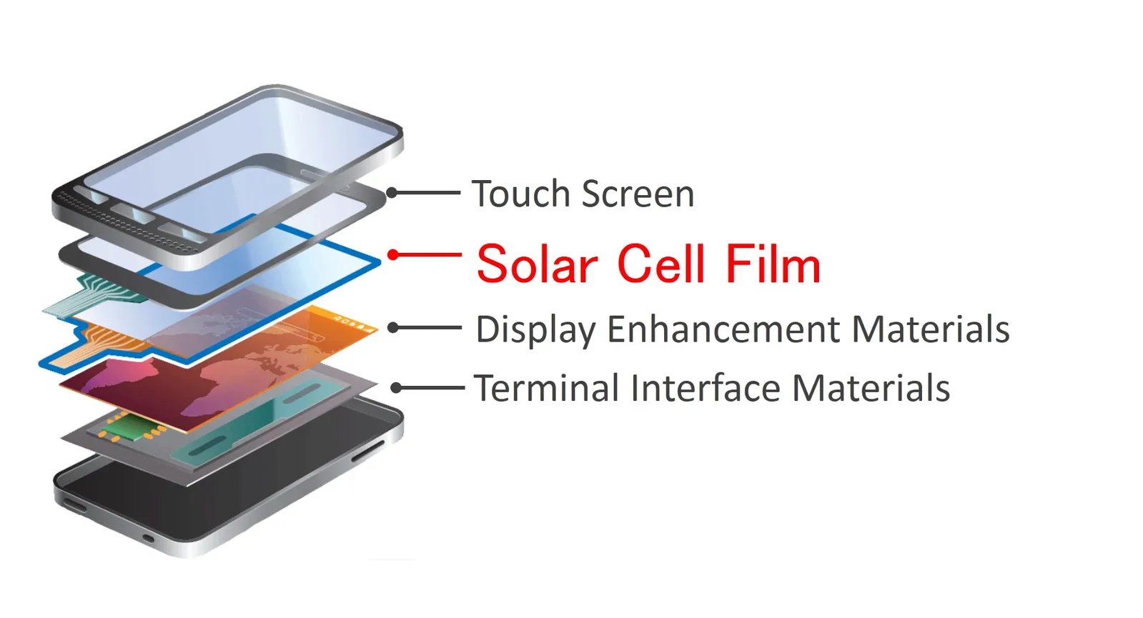
Deconstructing the Architecture: The In-Cell Advantage
To appreciate Kyocera's advancement, one must first understand the limitations of conventional touch displays. Most current devices utilize an additive design: a separate touch sensor panel (often using a technology like capacitive film) is laminated onto the surface of the LCD module. This "on-cell" or external touch layer approach, while effective, introduces inherent compromises. The extra layer adds physical thickness and weight, creates a small but perceptible air gap that can scatter light and reduce clarity, and can sometimes hinder touch sensitivity. Kyocera's in-cell technology dismantles this layered model. By embedding the touch sensing electrodes directly within the liquid crystal cell itself, the need for a discrete touch panel is eliminated. This integration is an engineering feat that simplifies the supply chain and assembly process while fundamentally altering the display's physical properties. The result is a more unified, efficient structure where the display and touch functionality are no longer separate entities but a single, cohesive system.
The Tangible Benefits: Slimmer Profiles and Enhanced Optics
The architectural shift from additive to integrated yields immediate and tangible benefits for end-user devices. The most obvious is a reduction in both thickness and weight. By removing the standalone touch layer and its associated adhesive films, displays can become significantly slimmer. This allows device OEMs to create remarkably thin smartphones, tablets, and laptops, or alternatively, allocate the saved space to larger batteries within the same chassis. Equally important is the dramatic improvement in image quality. The elimination of the air gap between the touch sensor and the LCD panel reduces internal light reflection and dispersion. This translates to higher contrast ratios, improved brightness efficiency, and vastly superior optical clarity, especially under bright ambient light. Text appears sharper, colors more vibrant, and videos more lifelike, as the image seems to be drawn directly on the glass surface, enhancing the perceived visual experience.
Beyond the Spec Sheet: Durability and Responsiveness
While slimness and image quality are headline features, Kyocera's in-cell technology delivers profound advantages in performance and reliability. The unified structure inherently improves mechanical durability. With fewer laminated layers, the display stack is less prone to delamination and more resistant to impacts and daily wear. Furthermore, the integrated design enhances touch sensitivity and responsiveness. The proximity of the sensing electrodes to the user's finger allows for more accurate signal detection, enabling better performance with gloved hands or in the presence of moisture—common pain points for traditional designs. This also paves the way for more consistent multi-touch performance and lower power consumption for the touch subsystem. For manufacturers, this means the ability to design more robust devices that feel premium and responsive, directly impacting user satisfaction and product longevity in competitive markets.
Kyocera's launch of in-cell touch display technology marks a pivotal moment in display engineering, moving beyond incremental tweaks to offer a holistic solution. By integrating touch sensors directly into the LCD cell, it successfully addresses the trilemma of thinness, image quality, and durability that has long constrained device designers. This innovation empowers OEMs to create下一代 devices that are not just slimmer and lighter, but also offer visually stunning, robust, and highly responsive interfaces. As this technology matures and scales, consumers can anticipate a new generation of electronics where the boundary between the user and the digital content becomes seamlessly imperceptible, fulfilling the enduring promise of technology that feels intuitively natural.


