In the fiercely competitive global display industry, a groundbreaking benchmark has been quietly shattered. Recent advancements from China have propelled Micro LED mass transfer technology into a new era, with reported efficiencies now exceeding 1,000 units per second.
In the fiercely competitive global display industry, a groundbreaking benchmark has been quietly shattered. Recent advancements from China have propelled Micro LED mass transfer technology into a new era, with reported efficiencies now exceeding 1,000 units per second. This isn't merely an incremental improvement; it's a quantum leap that fundamentally alters the economic and practical viability of Micro LED for mass-market applications.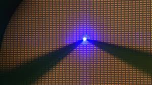
For years, the "transfer bottleneck"—the painstakingly slow process of moving millions of microscopic LED chips from a growth wafer to a target substrate—has been the single greatest barrier to Micro LED commercialization. Speeds measured in thousands of units per hour rendered large-screen displays prohibitively expensive. The achievement of a per-second transfer rate in the thousands unit range is therefore a seismic shift, signaling that the industry is moving from lab-scale prototyping toward genuine, scalable manufacturing.
The Engine of Revolution: Decoding the High-Speed Transfer Core
This monumental leap in speed is not accidental but stems from sophisticated engineering innovations. Traditional pick-and-place methods are entirely abandoned in favor of parallel transfer technologies. Techniques like laser-induced forward transfer (LIFT) or advanced stamp-based elastomer transfer act as pivotal enablers. These methods utilize a laser beam array or a meticulously engineered stamp with thousands of micro-cavities to capture, align, and release a vast array of Micro LEDs simultaneously in a single, swift action.
The magic lies in the parallelization. Instead of transferring one chip at a time, these systems transfer thousands in one "shot." Repeating this high-frequency cycle achieves the staggering >1000 UPS metric. Furthermore, this process integrates real-time, high-precision optical inspection and correction, ensuring that speed does not come at the cost of placement accuracy or yield. It represents a perfect marriage of precision mechanics, photonics, and intelligent control systems, creating the high-throughput engine that drives the entire new production paradigm.
From Lab to Market: Reshaping the Commercial Landscape
The commercial implications of this technological breakthrough are profound and immediate. First and foremost, it directly attacks the largest portion of Micro LED production cost: the transfer process. A hundred-fold increase in throughput translates to a dramatic reduction in cost per panel, moving Micro LED from the realm of luxury and niche products into the competitive space for high-end TVs, premium laptops, and automotive displays.
Secondly, it unlocks new product categories and form factors. With economically feasible high-speed transfer, creating large-area seamless video walls for control rooms or digital signage becomes practical. More importantly, it brings wearable devices—such as AR glasses requiring ultra-high-brightness, low-power micro-displays—closer to reality. The efficiency leap enables the mass production of the incredibly dense pixel arrays required for these next-generation applications, effectively accelerating the roadmap for the entire display ecosystem.
The Global Ripple Effect: Strategic and Supply Chain Implications
China's leadership in achieving this milestone sends ripples across the global technology and supply chain landscape. It signifies a strategic move from being a follower in display technology to a pioneer in core manufacturing equipment and processes. This capability grants Chinese panel makers and their downstream clients a significant first-mover advantage in launching next-generation display products.
On a global scale, this progress intensifies competition, compelling international players to accelerate their own R&D roadmaps. It also prompts a reevaluation of supply chain dynamics. The need for ultra-high-quality, uniform Micro LED epiwafers that are compatible with these blistering transfer speeds will increase, potentially reshaping the compound semiconductor supply chain. The race is no longer just about making better LEDs, but about perfecting the entire heterogeneous integration ecosystem—from chip epitaxy and testing to transfer and full-colorization—at an unprecedented pace and scale.
The breakthrough of exceeding 1000 Micro LED transfers per second is far more than a new speed record; it is the critical inflection point that transitions Micro LED from a promising technology to a commercially disruptive force. By mastering the core engine of parallel mass transfer, the industry has unlocked a path to scalable manufacturing, collapsing costs and enabling previously unimaginable applications. As this high-efficiency manufacturing capability matures and integrates with other key processes, it will catalyze a new wave of innovation across consumer electronics, professional visualization, and beyond, fundamentally reshaping what we expect from the screens in our lives.
1000 UPS metric. Furthermore, this process integrates real-time, high-precision optical inspection and correction, ensuring that speed does not come at the cost of placement accuracy or yield. It represents a perfect marriage of precision mechanics, photonics, and intelligent control systems, creating the high-throughput engine that drives the entire new production paradigm."}}},"align":"left","folded":false}},"doxcn0PcFR3gEJjt4AhBXiijjRe":{"id":"doxcn0PcFR3gEJjt4AhBXiijjRe","snapshot":{"type":"heading3","parent_id":"C4Lxdk6mpojip2xO8AKcRADpnqH","comments":null,"revisions":null,"locked":false,"hidden":false,"author":"7597729576936017103","children":[],"text":{"apool":{"nextNum":1,"numToAttrib":{"0":["author","7597729576936017103"]}},"initialAttributedTexts":{"attribs":{"0":"*0+1i"},"text":{"0":"From Lab to Market: Reshaping the Commercial Landscape"}}},"align":"left","folded":false}},"doxcnAX3yFrK4QWD14osOlmxMlb":{"id":"doxcnAX3yFrK4QWD14osOlmxMlb","snapshot":{"type":"text","parent_id":"C4Lxdk6mpojip2xO8AKcRADpnqH","comments":null,"revisions":null,"locked":false,"hidden":false,"author":"7597729576936017103","children":[],"text":{"apool":{"nextNum":1,"numToAttrib":{"0":["author","7597729576936017103"]}},"initialAttributedTexts":{"attribs":{"0":"*0+ca"},"text":{"0":"The commercial implications of this technological breakthrough are profound and immediate. First and foremost, it directly attacks the largest portion of Micro LED production cost: the transfer process. A hundred-fold increase in throughput translates to a dramatic reduction in cost per panel, moving Micro LED from the realm of luxury and niche products into the competitive space for high-end TVs, premium laptops, and automotive displays."}}},"align":"left","folded":false}},"doxcn9m4iQfKT6llzbYBVeG1pJd":{"id":"doxcn9m4iQfKT6llzbYBVeG1pJd","snapshot":{"type":"text","parent_id":"C4Lxdk6mpojip2xO8AKcRADpnqH","comments":null,"revisions":null,"locked":false,"hidden":false,"author":"7597729576936017103","children":[],"text":{"apool":{"nextNum":1,"numToAttrib":{"0":["author","7597729576936017103"]}},"initialAttributedTexts":{"attribs":{"0":"*0+fc"},"text":{"0":"Secondly, it unlocks new product categories and form factors. With economically feasible high-speed transfer, creating large-area seamless video walls for control rooms or digital signage becomes practical. More importantly, it brings wearable devices—such as AR glasses requiring ultra-high-brightness, low-power micro-displays—closer to reality. The efficiency leap enables the mass production of the incredibly dense pixel arrays required for these next-generation applications, effectively accelerating the roadmap for the entire display ecosystem."}}},"align":"left","folded":false}},"doxcnhBoZDulgaxa2cM5z6ycuYc":{"id":"doxcnhBoZDulgaxa2cM5z6ycuYc","snapshot":{"type":"heading3","parent_id":"C4Lxdk6mpojip2xO8AKcRADpnqH","comments":null,"revisions":null,"locked":false,"hidden":false,"author":"7597729576936017103","children":[],"text":{"apool":{"nextNum":1,"numToAttrib":{"0":["author","7597729576936017103"]}},"initialAttributedTexts":{"attribs":{"0":"*0+1t"},"text":{"0":"The Global Ripple Effect: Strategic and Supply Chain Implications"}}},"align":"left","folded":false}},"doxcnXcv6r47einfmpyCqt6IOLd":{"id":"doxcnXcv6r47einfmpyCqt6IOLd","snapshot":{"type":"text","parent_id":"C4Lxdk6mpojip2xO8AKcRADpnqH","comments":null,"revisions":null,"locked":false,"hidden":false,"author":"7597729576936017103","children":[],"text":{"apool":{"nextNum":2,"numToAttrib":{"0":["author","7597729576936017103"],"1":["italic","true"]}},"initialAttributedTexts":{"attribs":{"0":"*0+5h*0*1+1h*0+4d"},"text":{"0":"China's leadership in achieving this milestone sends ripples across the global technology and supply chain landscape. It signifies a strategic move from being a follower in display technology to a pioneer in core manufacturing equipment and processes. This capability grants Chinese panel makers and their downstream clients a significant first-mover advantage in launching next-generation display products."}}},"align":"left","folded":false}},"doxcnlGEDmebYgSU8pm2ZGUqadf":{"id":"doxcnlGEDmebYgSU8pm2ZGUqadf","snapshot":{"type":"text","parent_id":"C4Lxdk6mpojip2xO8AKcRADpnqH","comments":null,"revisions":null,"locked":false,"hidden":false,"author":"7597729576936017103","children":[],"text":{"apool":{"nextNum":2,"numToAttrib":{"0":["author","7597729576936017103"],"1":["bold","true"]}},"initialAttributedTexts":{"attribs":{"0":"*0+d0*0*1+p*0+32"},"text":{"0":"On a global scale, this progress intensifies competition, compelling international players to accelerate their own R&D roadmaps. It also prompts a reevaluation of supply chain dynamics. The need for ultra-high-quality, uniform Micro LED epiwafers that are compatible with these blistering transfer speeds will increase, potentially reshaping the compound semiconductor supply chain. The race is no longer just about making better LEDs, but about perfecting the entire heterogeneous integration ecosystem—from chip epitaxy and testing to transfer and full-colorization—at an unprecedented pace and scale."}}},"align":"left","folded":false}},"doxcnKf5Txawa0q1ZQf0TBLc7hb":{"id":"doxcnKf5Txawa0q1ZQf0TBLc7hb","snapshot":{"type":"text","parent_id":"C4Lxdk6mpojip2xO8AKcRADpnqH","comments":null,"revisions":null,"locked":false,"hidden":false,"author":"7597729576936017103","children":[],"text":{"initialAttributedTexts":{"text":{"0":"The breakthrough of exceeding 1000 Micro LED transfers per second is far more than a new speed record; it is the critical inflection point that transitions Micro LED from a promising technology to a commercially disruptive force. By mastering the core engine of parallel mass transfer, the industry has unlocked a path to scalable manufacturing, collapsing costs and enabling previously unimaginable applications. As this high-efficiency manufacturing capability matures and integrates with other key processes, it will catalyze a new wave of innovation across consumer electronics, professional visualization, and beyond, fundamentally reshaping what we expect from the screens in our lives."},"attribs":{"0":"*0+j8"}},"apool":{"numToAttrib":{"0":["author","7597729576936017103"]},"nextNum":1}},"align":"left","folded":false}},"C4Lxdk6mpojip2xO8AKcRADpnqH":{"id":"C4Lxdk6mpojip2xO8AKcRADpnqH","snapshot":{"type":"page","parent_id":"","comments":[],"revisions":[],"locked":false,"hidden":false,"author":"7597729576936017103","children":["doxcnJLn7aSykW36M4BoU4N3HFe","doxcnbRAdHKEg3vDrhHbMznNxJf","doxcnpwnNmjTWIRcHFEi6sIa43d","doxcnaGEwsEkWvXneIibWw64SHd","doxcnxH3NDacAe65F7tkRwJ0x7b","doxcn0PcFR3gEJjt4AhBXiijjRe","doxcnAX3yFrK4QWD14osOlmxMlb","doxcn9m4iQfKT6llzbYBVeG1pJd","doxcnhBoZDulgaxa2cM5z6ycuYc","doxcnXcv6r47einfmpyCqt6IOLd","doxcnlGEDmebYgSU8pm2ZGUqadf","doxcnKf5Txawa0q1ZQf0TBLc7hb"],"text":{"apool":{"nextNum":1,"numToAttrib":{"0":["author","7597729576936017103"]}},"initialAttributedTexts":{"attribs":{"0":"*0+1b"},"text":{"0":"Micro LED Mass Transfer Hits 1000+ Units/Second"}}},"align":"","doc_info":{"editors":["7597729576936017103"],"options":["editors","edit_time"],"deleted_editors":null,"option_modified":null}}}},"payloadMap":{"doxcnJLn7aSykW36M4BoU4N3HFe":{"level":1},"doxcnbRAdHKEg3vDrhHbMznNxJf":{"level":1},"doxcnaGEwsEkWvXneIibWw64SHd":{"level":1},"doxcnxH3NDacAe65F7tkRwJ0x7b":{"level":1},"doxcnAX3yFrK4QWD14osOlmxMlb":{"level":1},"doxcn9m4iQfKT6llzbYBVeG1pJd":{"level":1},"doxcnXcv6r47einfmpyCqt6IOLd":{"level":1},"doxcnlGEDmebYgSU8pm2ZGUqadf":{"level":1},"doxcnKf5Txawa0q1ZQf0TBLc7hb":{"level":1},"lingoClipboardPayload":{"spaceSubExtraInfo":[{"spaceSubId":"doxcnxH3NDacAe65F7tkRwJ0x7b","word":"paradigm"},{"spaceSubId":"doxcn9m4iQfKT6llzbYBVeG1pJd","word":"AR"}],"spaceId":"C4Lxdk6mpojip2xO8AKcRADpnqH","spaceType":1}},"extra":{"channel":"saas","pasteRandomId":"8c281a98-7e16-4cfe-8d85-e80a9f42d161","mention_page_title":{},"external_mention_url":{},"isEqualBlockSelection":true},"isKeepQuoteContainer":false,"selection":[{"id":2,"type":"text","selection":{"start":0,"end":441},"recordId":"doxcnJLn7aSykW36M4BoU4N3HFe"},{"id":3,"type":"text","selection":{"start":0,"end":534},"recordId":"doxcnbRAdHKEg3vDrhHbMznNxJf"},{"id":4,"type":"text","selection":{"start":0,"end":63},"recordId":"doxcnpwnNmjTWIRcHFEi6sIa43d"},{"id":5,"type":"text","selection":{"start":0,"end":534},"recordId":"doxcnaGEwsEkWvXneIibWw64SHd"},{"id":6,"type":"text","selection":{"start":0,"end":569},"recordId":"doxcnxH3NDacAe65F7tkRwJ0x7b"},{"id":7,"type":"text","selection":{"start":0,"end":54},"recordId":"doxcn0PcFR3gEJjt4AhBXiijjRe"},{"id":8,"type":"text","selection":{"start":0,"end":442},"recordId":"doxcnAX3yFrK4QWD14osOlmxMlb"},{"id":9,"type":"text","selection":{"start":0,"end":552},"recordId":"doxcn9m4iQfKT6llzbYBVeG1pJd"},{"id":10,"type":"text","selection":{"start":0,"end":65},"recordId":"doxcnhBoZDulgaxa2cM5z6ycuYc"},{"id":11,"type":"text","selection":{"start":0,"end":407},"recordId":"doxcnXcv6r47einfmpyCqt6IOLd"},{"id":12,"type":"text","selection":{"start":0,"end":603},"recordId":"doxcnlGEDmebYgSU8pm2ZGUqadf"},{"id":13,"type":"text","selection":{"start":0,"end":692},"recordId":"doxcnKf5Txawa0q1ZQf0TBLc7hb"}],"pasteFlag":"3933681f-0436-4342-8b6b-d8ca62a7f24e"}" data-lark-record-format="docx/record" class="lark-record-clipboard" style="font-size: 16px;">


